The global etching chemicals market is closely tied to semiconductor fabrication,
printed circuit board production, metal treatment, glass processing, MEMS,
advanced packaging and other precision manufacturing activities where controlled removal of material is required. The industry uses a broad chemical base that includes hydrofluoric acid, hydrochloric acid,
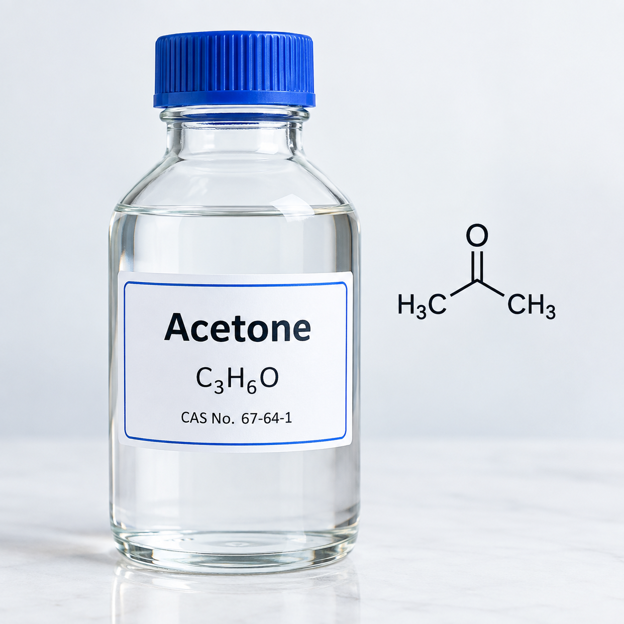
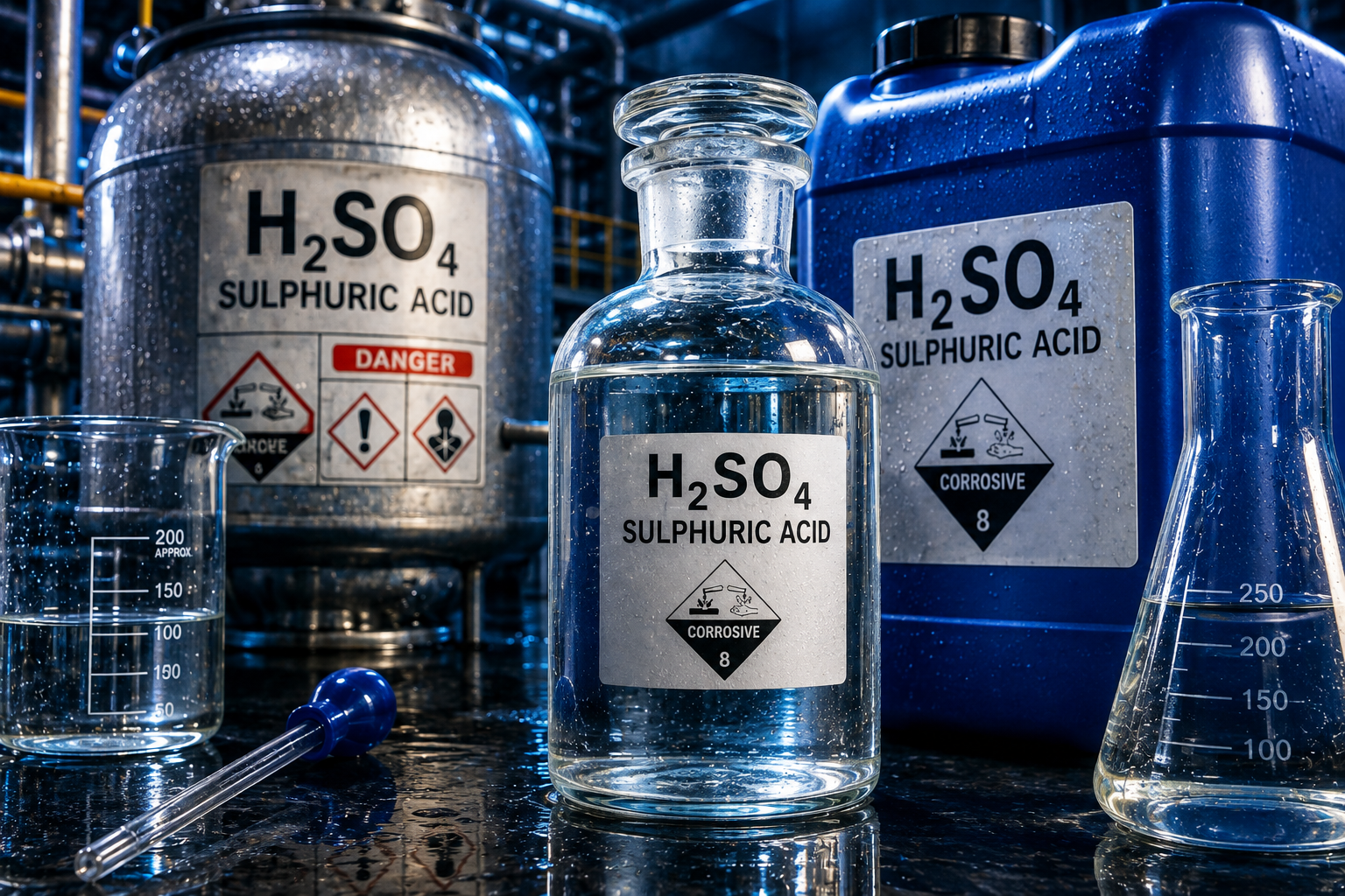
nitric acid, sulfuric acid, phosphoric acid, hydrogen peroxide, ammonium hydroxide, ferric chloride and formulated mixtures, while
semiconductor manufacturing increasingly requires ultra-high purity grades with tightly controlled metallic and particulate contamination. Regulation is therefore an important part of the market because many commonly used etchants are corrosive, toxic or environmentally hazardous. In the United States, chemical manufacturers and importers operate under the Toxic Substances Control Act (TSCA), including Chemical Data Reporting requirements covering production, importation and use information. EPA's latest CDR release provides information on chemicals manufactured or imported into the U.S. during 2020-2023, demonstrating the importance of regulatory monitoring across chemical supply chains. Hydrogen fluoride is particularly relevant because EPA included it among 16 chemicals subject to additional health and safety study reporting requirements under TSCA Section 8(d), with the reporting deadline subsequently extended to May 21, 2027.In addition and manufacturing facilities must address applicable air emission, wastewater, hazardous material handling, worker safety and hazardous waste requirements at federal, state and local levels. The regulatory direction is creating opportunities for suppliers that can provide higher purity chemicals, safer formulations, improved chemical delivery systems, lower emission processes, recycling technologies and alternatives to chemicals facing tighter environmental scrutiny.
According to the research report "Global Etching Chemicals Market Outlook, 2031," published by Bonafide Research, the Global Etching Chemicals Market was valued at more than USD 10.42 Billion in 2025, and expected to reach a market size of more than USD 14.77 Billion by 2031 with the CAGR of 6.15% from 2026-2031.The transaction illustrates a broader industry trend toward combining chemical formulation expertise with local manufacturing,
logistics and total chemical management services. At the same time, Mitsubishi Gas Chemical expanded its Texas production facility operated by MGC Pure Chemicals America for super pure hydrogen peroxide and ammonium hydroxide. These materials are used in semiconductor cleaning, etching and related wafer processing applications, showing how producers are localizing critical chemical capacity near North American fabs rather than relying entirely on long distance imports. Raw material supply remains an important consideration because etching formulations depend on industrial acids, bases, oxidizers,
solvents, ultrapure water and specialty additives, while semiconductor grade products require additional purification and contamination control steps. International trade consequently remains an integral part of the industry even as governments promote regional manufacturing. Chemical suppliers frequently use globally distributed production networks in which base chemicals or intermediates can be produced in one country, purified or formulated elsewhere, and then supplied to semiconductor and electronics customers in another region. A significant development has been the expansion of MGC Pure Chemicals America's Texas facility, which manufactures super pure hydrogen peroxide and ammonium hydroxide used in semiconductor processing. Mitsubishi Gas Chemical announced the Texas expansion in 2024, emphasizing that these materials are used for cleaning, etching and abrasion-related processes in
semiconductor wafer and device manufacturing.
Oxidizing etchants are gaining strong importance because oxidation is a fundamental step in many wet-chemical etching reactions, particularly where the material being removed must first be chemically converted before it can dissolve from the
surface. In practical etching systems, hydrogen peroxide and nitric acid are commonly used as oxidizing components, while other chemicals such as hydrochloric acid, hydrofluoric acid, ammonium hydroxide, or phosphoric acid can support the subsequent dissolution stage. This reaction sequence gives oxidizing chemistries considerable flexibility across different materials and process environments. Nitric acid, for example, is used as an oxidizing ingredient in etching mixtures for
copper, silver,
aluminum, silicon, germanium and, in combination with hydrochloric acid, gold, demonstrating that one oxidizing chemistry can serve multiple material-processing requirements. This broad material compatibility is particularly relevant to electronics manufacturing, where different fabrication steps involve copper, aluminum, titanium, nickel and other metals. Semiconductor chemical suppliers also maintain dedicated wet-etching portfolios for aluminum, copper, nickel, titanium and metal stacks, showing that wet etching remains relevant for several layers and structures within advanced device manufacturing. Hydrogen peroxide provides another important route because it is incorporated into several established semiconductor and microelectronics chemistries, including Piranha type etching solutions, RCA related cleaning chemistries and etching systems for III/V
semiconductor materials.
Wet etching remains a leading etching process because it combines a mature chemical-processing method with broad material compatibility and practical production advantages. The process works by bringing a liquid chemical solution into direct contact with the exposed material, allowing the targeted layer to react and dissolve while a photoresist, oxide, or other masking layer protects areas that need to remain. IEEE describes wet etching as particularly useful where high selectivity, large batch throughput, and relatively smooth surfaces are important, which explains its continued use even though dry etching has become essential for highly scaled semiconductor structures. One of the most important advantages is selectivity: manufacturers can formulate an etchant to attack a particular material while minimizing reaction with adjacent layers. This is especially valuable in semiconductor processing, where wafers contain multiple thin films and different materials that must be removed sequentially without unnecessarily damaging neighboring structures. Wet processing is also used for native oxide removal, organic residue cleaning, surface preparation, and selective layer removal, meaning its role extends beyond a single pattern transfer operation. Another factor is throughput. Liquid etching can process relatively large surface areas simultaneously, and conventional batch systems can treat multiple wafers in a common chemical environment, while single wafer wet systems are used when tighter process control is required. Wet chemistry also plays a significant role outside semiconductor fabrication. In PCB manufacturing, chemical etching is widely used to remove unwanted copper from conductive layers and form the required circuit pattern, with ferric chloride and cupric chloride among established etching chemistries.
Printed circuit boards maintain steady demand for etching chemicals because copper circuit formation is fundamentally dependent on controlled chemical removal during several established PCB fabrication routes. A PCB begins with a nonconductive substrate carrying
copper foil, and the circuit pattern is created by protecting the copper that must remain while chemically removing the exposed copper areas. This makes etching an integral part of converting a copper clad panel into functional electrical interconnections rather than an optional finishing operation. The process is particularly suitable for PCB production because large panels can be processed using conveyorized or spray based equipment, allowing manufacturers to treat substantial surface areas consistently. In commercial PCB production, commonly used chemistries include cupric chloride, ammonium based etchants, ferric chloride, and persulfate systems, with the selected chemistry depending on the layer structure, resist system, copper thickness, and required process conditions. Cupric chloride is especially established in PCB fabrication because it provides a high etching rate and can be regenerated, while ammonium based systems is used for particular outer layer processing requirements. The importance of etching is also connected to the increasing technical complexity of circuit boards. Modern boards can contain multiple conductive layers, fine circuit geometries, plated features, and high density interconnections, requiring close control over etch time, temperature, chemical concentration, spray conditions, and copper loading. IPC technical material highlights that reducing copper removal during controlled micro etching can be important for fine line and controlled impedance inner layer manufacturing, demonstrating how chemical control becomes more demanding as PCB designs become more sophisticated.







 We are friendly and approachable, give us a call.